- HOME
- Product information
- CYTOP™
- CYTOP™ Usage
Usage

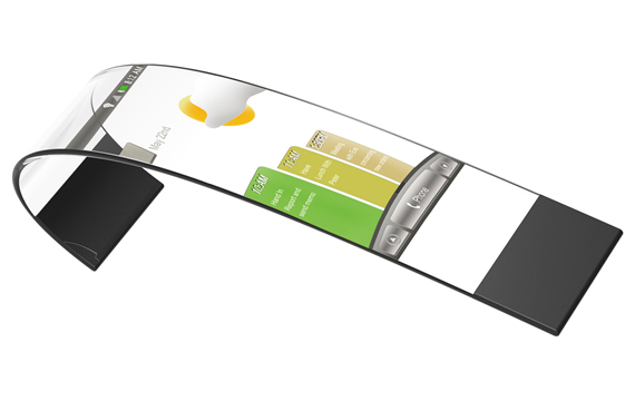
Gate insulators for organic semiconductors in flexible displays
Because CYTOP™ is an “insulating material” that has good “compatibility with organic semiconductors” and can withstand “flexibility”, it is used in many research institutes as a “gate insulator” in flexible displays that are thin, light, and flexible.
Click here for details

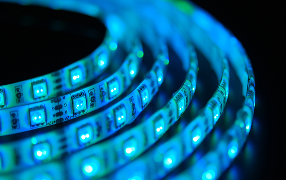
Deep-UV LED encapsulants
CYTOP™ is focused on as a material for use in “Deep-UV LED encapsulants” for its transparency and also due to its durability as compared to epoxy resins and silicon resins. One CYTOP™ application is “pellicles” on photomasks preventing particle contamination. This “pellicle” is a vital material for the exposure process of semiconductor manufacturing, and since they are in an environment that is irradiated with exposure wavelength ArF (193nm) and KrF (248nm), CYTOP™ is considered as an encapsulant material in UV-C (200-280nm) LEDs.
Click here for details

Electret material for vibration power generators
Energy harvesting is a technology that can extract a tiny amount of unused energy as electricity. Vibration, light and heat can be used as energy sources for energy harvesting, and because CYTOP™ has the ability to keep a charge (=electret property) semipermanently , it is used as a “vibration power generator material”. As long as there is vibration, maintenance-free ultra small vibration power generators which do not require battery replacement or charging is expected to be untilized as power sources for sensors in IoT devices.
Click here for details

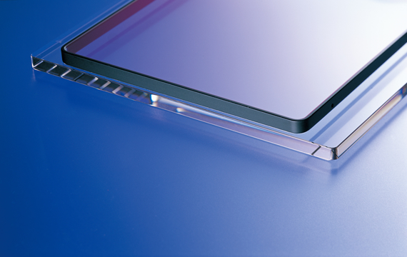
“Pellicle” is a thin film on photomasks preventing particle contamination
A “pellicle” is a product that prevents the reduction in production yield during the exposure process in semiconductor manufacturing. “Pellicles” are vital materials in the exposure process in semiconductor manufacturing, and they are used in an environment that is irradiated with exposure wavelength ArF (193nm) and KrF (248nm). Since CYTOP™ has the rare characteristic of also transmitting deep UV light, it is used as a material in “pellicles”.
Click here for details

Ultrafast plastic optical fiber “Fontex”
By adopting CYTOP™, “Fontex” is more resistant to bending than quartz and ultra high speed transmission is possible. Optical fiber that uses acrylic resin experiences transmission loss in optical communication in the 650nm-1300nm wavelength region due to the C-H bonds contained in the acrylic resin. However “Fontex” using CYTOP™ does not contain C-H bonds, so the 650nm-1300nm region is transparent and there is virtually no transmission loss. Compared to copper wire, it is lightweight with low power consumption and is resistant to noise.
Click here for details

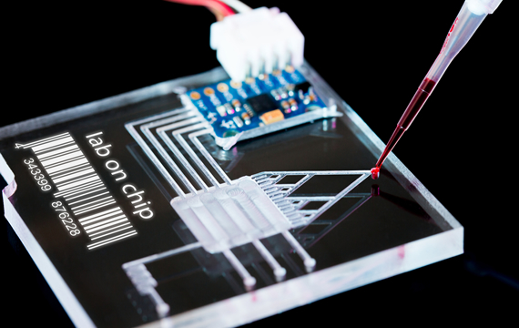
“Biochips” for detecting cells, DNA, and proteins
In addition to the properties of “chemical resistance”, “liquid repellency”, and “low adhesion with biological materials” that are necessary for “biochips”, and since CYTOP™ has characteristics of “low autofluorescence”, and “nearly the same refractive index as water (1.34)”, it is easy to view with a microscope. Furthermore, by making use of the property of “wettability control” which employs the electrowetting phenomenon with the on/off of voltage, it is possible to move, separate and mix microscopic droplets.
Click here for details


